
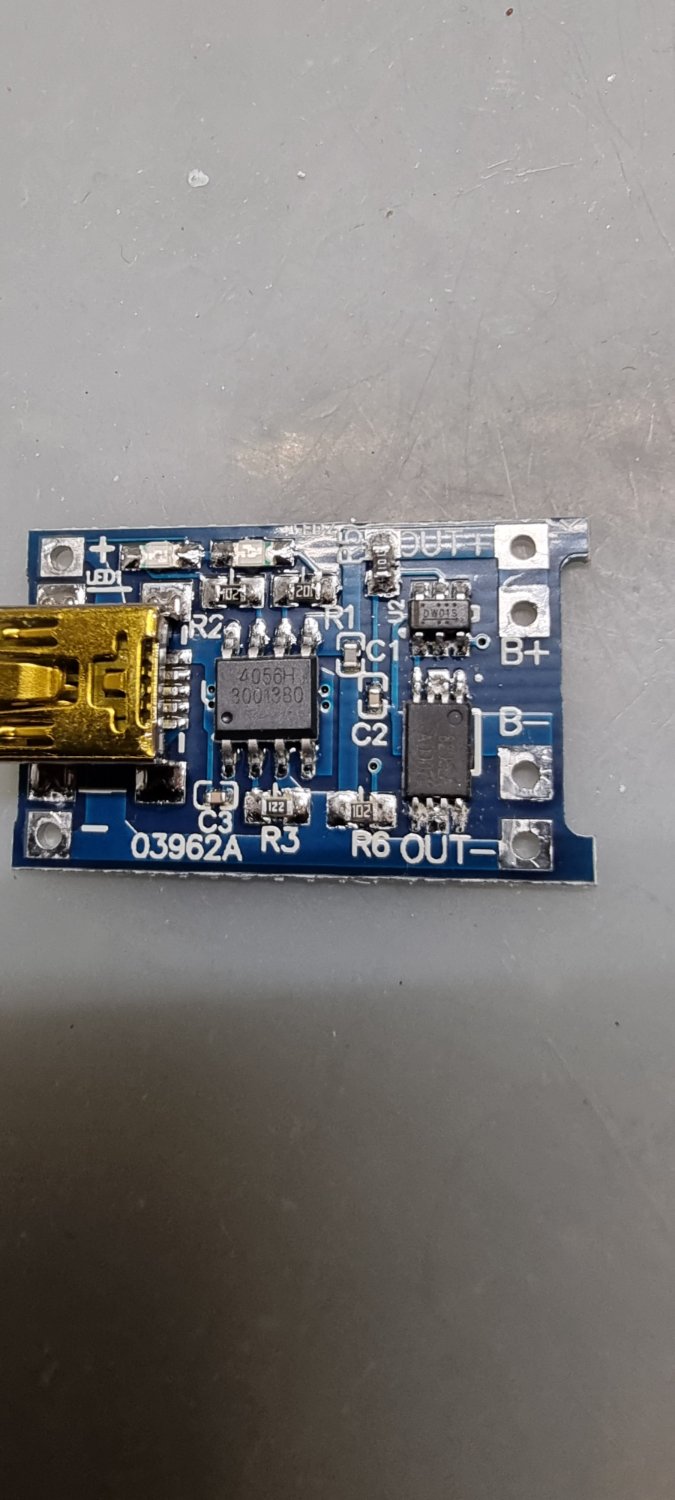
I got these TP4056 modules from an AliExpress vendor and fail to understand how the protection circuit works or if it’s just typical Ali shovelware. It could be my limited understanding of electronics.
The protection circuit appears to be just for show. To the right there’s a DW01S chip that prevents over charging and discharging in combination with the 8205 dual channel MOSFET.
It looks like the drain of this MOSFET isn’t connected anywhere. I’ve tried following the traces using a multimeter and no other pin shows continuity with the drain. Source1 is connected to Battery - and Source2 is connected to Terminal -.
I suppose the Drain starts participating in the circuit when one mosfet activates.
What was the idea behind this? That the 8205 acts as an AND gate by having them both in series?
I’m trying to make an 18650 testing circuit that uses these modules to charge and discharge a battery and wanted to use the protection circuit mosfet as a trigger for discharging.
The MOSFETs are in series, but in opposite polarities. Two MOSFETs are needed to block current in both directions.
The DW01 uses the voltage drop across the MOSFETS to measure the current. The overcurrent threshold voltage is fixed at 150mV. Using a larger MOSFET that has a lower RDS(on) will increase the current limit.